TRUE-ONE FPGA DEVELOPMENT BOARD
TRUE-ONE FPGA DEVELOPMENT BOARD MANUAL
The TRUE-ARTDAC7 FPGA Development Board is a domestically produced FPGA development platform designed for developing high-performance digital designs and embedded system applications. Developed based on the AMD Xilinx Artix-7 architecture, the board provides the fundamental infrastructure required for education, R&D, rapid prototyping, and hardware verification on a single platform.
Featuring a user-friendly structure, TRUE-ARTDAC7 allows for the development and testing of numerous FPGA-based applications without the need for additional hardware, thanks to its onboard peripheral hardware and user input/output units. The programming interfaces, memory structure, and expansion headers on the board offer a suitable environment for both entry-level applications and more advanced development studies.
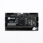
The board features the XC7A50T-1FTG256C FPGA chip. Additionally, voltage levels of 1.0 V, 1.8 V, and 3.3 V are used within the system structure. Its compact dimensions of 14 cm × 8 cm provide a suitable mechanical infrastructure for desktop work, laboratory use, educational applications, and product demonstration processes.
Artix-7 Based FPGA Development Board with DAC Module Support
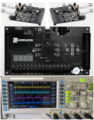
The TRUE-ARTDAC7 FPGA Development Board is a domestically produced FPGA development platform designed for developing high-performance digital designs and embedded system applications. It operates in full compatibility with the Xilinx Vivado Design Suite. By using the two 40-pin headers on the TRUE-ARTDAC7 FPGA Development Board, digital signals processed or generated on the FPGA can be converted into analog signals via the DAC module (each DAC module enables the conversion of two digital signals). These signals can then be visualized with an oscilloscope or used to control various systems.
Highlights
The board features the XC7A50T-1FTG256C FPGA chip from the Artix-7 family produced by AMD (Xilinx). Thanks to its low power consumption and high processing capacity, this chip offers a flexible field of use in both educational and R&D projects. Its extensive logic resources and DSP blocks allow for the realization of complex digital designs and high-speed data processing applications.
|
TRUE-ARTDAC7 FPGA DEVELOPMENT BOARD |
|
|
FPGA Chip |
XC7A50T-1FTG256C |
|
Logic Cell |
8,150 slices and 52,160 logic cells (each slice contains four 6-input LUTs and 8 flip-flops) |
|
Block RAM |
2,700 Kbits of fast block RAM and five clock management tiles, each featuring a phase-locked loop (PLL) |
|
DSP Slices |
120 |
|
Internal Clock Speed |
450 MHz+ |
|
Quad-SPI Flash |
4 MB |
|
CONNECTION / INTERFACE |
|
|
• FT2232HL: JTAG + USB-UART |
|
|
ONBOARD I/O |
|
|
• 100 MHz External Clk Frequency |
|
|
POWER SUPPLY |
|
|
Input |
5 V (Micro USB) |
|
Output |
5 V (DC Jack Adaptör) |
|
PHYSICAL |
|
|
Dimensions |
80 mm × 140 mm |
|
AREAS OF USAGE |
|
|
• Digital Signal Processing and Prototyping |
|