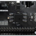
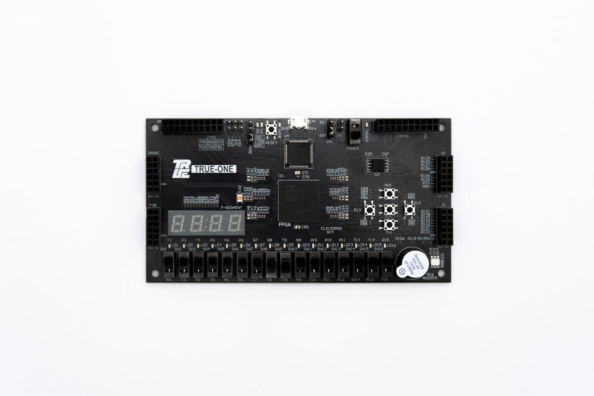
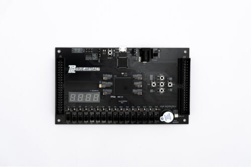
The TRUE-ONE FPGA Development Board is a domestically produced FPGA development platform designed for developing high-performance digital designs and embedded system applications. Developed based on the AMD Xilinx Artix-7 architecture, the board provides the fundamental infrastructure required for education, R&D, rapid prototyping, and hardware verification on a single platform.
Featuring a user-friendly structure, TRUE-ONE allows for the development and testing of numerous FPGA-based applications without the need for additional hardware, thanks to its onboard peripheral hardware and user input/output units. The programming interfaces, memory structure, and expansion headers on the board offer a suitable environment for both entry-level applications and more advanced development studies.
The board features the XC7A50T-1FTG256C FPGA chip. Additionally, voltage levels of 1.0 V, 1.8 V, and 3.3 V are used within the system structure. Its compact dimensions of 13 cm × 7 cm provide a suitable mechanical infrastructure for desktop work, laboratory use, educational applications, and product demonstration processes.
Artix-7 Based FPGA Development Board
The TRUE-ONE FPGA Development Board is a domestically produced FPGA development platform designed for developing high-performance digital designs and embedded system applications. It operates in full compatibility with the Xilinx Vivado Design Suite. Featuring a user-friendly architecture, the TRUE-ONE FPGA Development Board is equipped with numerous different inputs/outputs and various peripheral units. Thus, it provides users with the opportunity to fully develop and run many FPGA-based designs without the need for any additional hardware.
Highlights
The board features the XC7A50T-1FTG256C FPGA chip from the Artix-7 family produced by AMD (Xilinx). Thanks to its low power consumption and high processing capacity, this chip offers a flexible field of use in both educational and R&D projects. Its extensive logic resources and DSP blocks allow for the realization of complex digital designs and high-speed data processing applications.
The TRUE-ONE board also includes dedicated XADC pin headers reserved for the user to utilize the FPGA chip's internal analog-to-digital converter (XADC). This structure makes it possible to develop data acquisition and real-time analog analysis applications by directly connecting external analog sensors and measurement circuits to the FPGA chip.
|
TRUE-ONE FPGA DEVELOPMENT BOARD |
|
|---|---|
| FPGA Chip | XC7A50T-1FTG256C |
| Logic Cell | 8,150 slices and 52,160 logic cells (each slice contains four 6-input LUTs and 8 flip-flops) |
| Block RAM | 2,700 Kbits of fast block RAM and five clock management tiles, each featuring a phase-locked loop (PLL) |
| DSP Slices Count | 120 |
| Internal Clock Speed | 450 MHz+ |
| Quad-SPI Flash | 128 MB |
| CONNECTION / INTERFACE | |
| • FT2232HL: JTAG + USB-UART • Micro USB 2.0 |
|
| ONBOARD I/O | |
|
• 100 MHz External Clk Frequency |
|
| POWER SUPLY | |
| Input | 5 V (Micro USB) |
| Output | 5 V (Pin Header) |
| PHYSICAL | |
| Dimensions | 70 mm × 130 mm |
| AREAS OF USAGE | |
| • Digital Signal Processing and Prototyping • FPGA Education and Laboratory Studies • Rapid I/O Development and Testing |
|