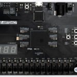
1. Product Overview
The TRUE-ONE FPGA Development Board is a locally produced FPGA development platform designed for high-performance digital designs and embedded system applications. Built upon the AMD Xilinx Artix-7 architecture, the board provides the essential infrastructure required for education, R&D, rapid prototyping, and hardware verification on a single platform.
Featuring a user-friendly design, TRUE-ONE allows for the development and testing of numerous FPGA-based applications without the need for additional hardware, thanks to its onboard peripherals and user I/O units. The programming interfaces, memory structure, and expansion headers on the board provide a suitable environment for both entry-level applications and more advanced development projects.
The board features the XC7A50T-1FTG256C FPGA chip. Additionally, the system architecture utilizes voltage levels of 1.0 V, 1.8 V, and 3.3 V. Its compact 13 cm × 7 cm physical footprint provides a convenient mechanical infrastructure for desktop work, laboratory use, educational applications, and product demonstration processes.
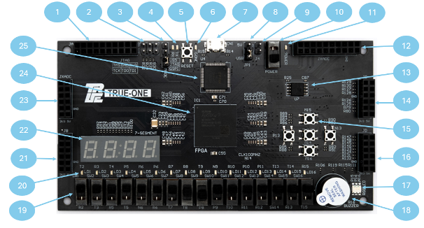
| No. | Component | No. | Component |
| 1 | 2x20 JA Pin Header | 14 | 2x6 JC Pin Header |
| 2 | JTAG Programming | 15 | Push Button |
| 3 | Programming Mode | 16 | 2x6 JD Pin Header |
| 4 | RX/TX LED | 17 | RGB LED |
| 5 | Reset Button | 18 | Buzzer |
| 6 | Done LED | 19 | User Switch |
| 7 | UART/JTAG USB Port | 20 | User LED |
| 8 | Power Mode | 21 | 2x6 JB Pin Header |
| 9 | External Supply | 22 | 7-Segment |
| 10 | Power Switch | 23 | 2x6 JXADC Pin Header |
| 11 | Power LED | 24 | FPGA XC7A50T-1FTG256C |
| 12 | 2x20 JXADC Pin Header | 25 | FTDI FT2232HL-REEL |
| 13 | QSPI FLASH |
| No. | Component | No. | Component |
| 1 | JTAG Programming | 11 | Push Button |
| 2 | Programming Mode | 12 | 2x40 DAC Pin Header |
| 3 | RX/TX LED | 13 | User LED |
| 4 | Reset Button | 14 | Buzzer |
| 5 | Done LED | 15 | RGB LED |
| 6 | UART/JTAG USB Port | 16 | User Switch |
| 7 | Power Mode | 17 | 7-Segment |
| 8 | External Supply | 18 | 2x40 DAC Pin Header |
| 9 | Power Switch | 19 | FPGA XC7A50T-1FTG256C |
| 10 | Power LED |
2. FPGA CHIP
The TRUE-ONE FPGA development board features the XC7A50T-1FTG256C FPGA chip from the AMD Xilinx Artix-7 family. This FPGA chip provides a suitable infrastructure for education, R&D, prototyping, and digital design applications, thanks to its architecture that combines high performance with low power consumption.
The XC7A50T model enables the implementation of numerous FPGA-based applications with its logic resources, block RAM capacity, DSP units, and internal analog-to-digital converter structure. The FTG256 package preferred on the board offers sufficient I/O capacity for compact board designs while providing an advantage in terms of board layout.
The Artix-7 FPGA chip used on the TRUE-ONE board offers a robust hardware infrastructure for controlling user I/O units, timing-based designs, communication applications, digital signal processing studies, and developments carried out with external modules.
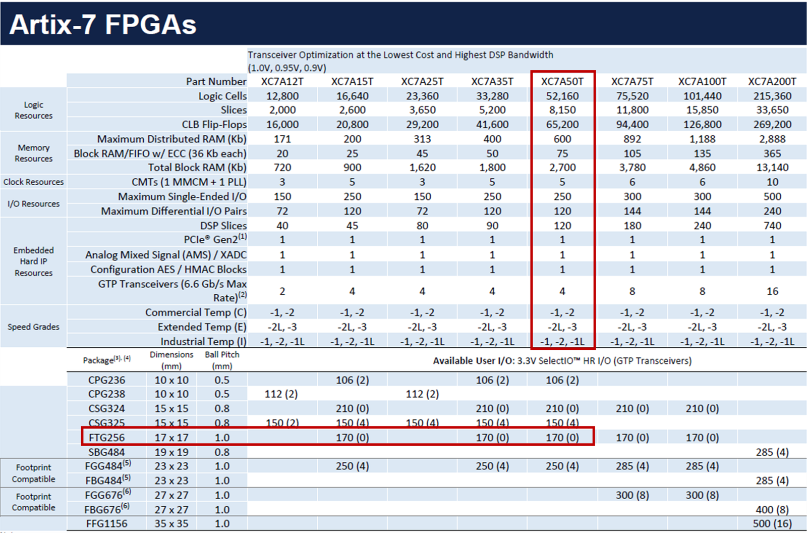
Figure 2- 1: Features of the Utilized FPGA Family
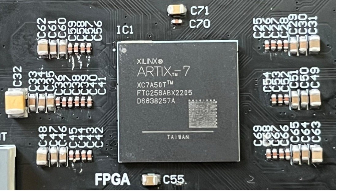
Figure 2- 2: Chip Located on the Board
3. Power Architecture and Supply Structure
The TRUE-ONE FPGA development board generates the necessary operating voltages through an onboard power regulation structure. The board's supply architecture is designed to provide the essential voltage levels required by the FPGA chip and its peripherals in a stable and secure manner.
There are three main supply lines on the board: 1.0 V, 1.8 V, and 3.3 V. These voltages are used respectively for the FPGA core architecture, auxiliary supply lines, and the operation of input/output peripherals.
The board's power-on sequence is designed according to a sequential activation logic. Upon receiving the activation signal from the power switch, the 1.0 V regulator is engaged first. Subsequently, the 1.8 V regulator is activated using the Power Good (PG) output of the previous regulator. In the final stage, the 3.3 V supply line is generated. This structure ensures that power rails are established in a controlled order, allowing the system to start up stably.
The power converters used on the board are from the TPS56628DDAR series. Each regulator is configured to produce its respective voltage line.
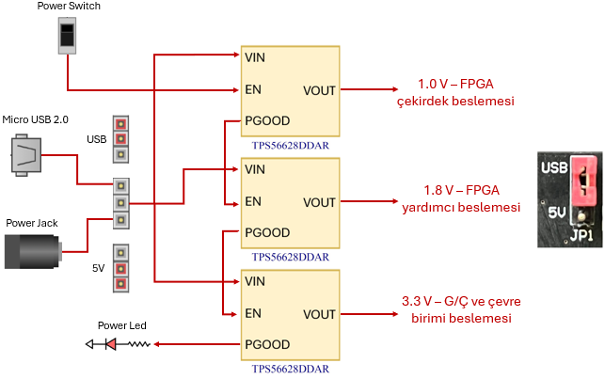
Figure 3- 1: TRUE-ONE Power Architecture Block Diagram
4. Configuration Modes
After power is applied, the Artix-7 FPGA chip on the TRUE-ONE FPGA development board must be programmed with a configuration file to become functional. This configuration data is a bitstream file that defines the logic functions and circuit connections to be implemented within the FPGA. This file, created in the Vivado design environment, can be uploaded to the board using different methods.
In JTAG configuration, the bitstream file is uploaded directly from the computer to the FPGA chip using the USB-JTAG interface. This method provides a fast and practical use during the development and debugging processes. However, configuration uploaded this way is volatile; the logic structure inside the FPGA is lost when the board's power is disconnected.
In QSPI Flash configuration, the bitstream file is written to the non-volatile flash memory located on the board. Upon power-up, the FPGA reads the data stored in this memory under the appropriate configuration settings and initializes automatically. This method is suitable for permanent applications, demonstrations, and scenarios requiring an automatic start at every power-on. The configuration options and related hardware structure for the TRUE-ONE board are shown below.
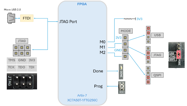
Figure 4- 1: Connection Structure of TRUE-ONE Configuration Modes
5. Clock Source
The TRUE-ONE FPGA development board features an oscillator with a frequency of 100 MHz as the system clock source. The oscillator model used on the board is the ASEM1-100.000MHZ-LC-T. This oscillator is integrated into the board to be used as the FPGA clock input in designs.
Depending on the application being developed, different frequencies can be derived from this 100 MHz input clock by utilizing the clock management resources (such as MMCMs or PLLs) within the FPGA chip. This allows for the generation of various operating frequencies required by the specific design.
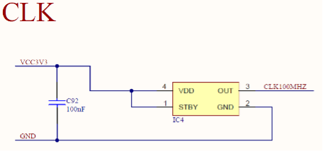
Figure 5- 1: TRUE-ONE System Clock Block Diagram
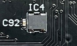
Figure 5- 2: Oscillator Located on the Board
Table 5- 1: CLK Pin Assignment
|
CLK Pin Name |
FPGA Pin Name |
FPGA Pin |
|
CLK100MHZ |
IO_L12P_T1_MRCC_14 |
N14 |
6. QSPI Flash Memory
The TRUE-ONE FPGA development board features a 128 Mbit capacity QSPI Flash memory for system configuration and non-volatile data storage. The specific flash memory model used is the Micron MT25QL128ABA1ESE-0SIT, operating at a 3.3 V CMOS logic level.
Thanks to its non-volatile nature, the QSPI Flash memory is primarily used to store FPGA configuration data. With the appropriate mode settings, the FPGA can automatically read and initialize from the bitstream file stored in this memory upon power-up. This architecture ensures that designs are not limited to temporary volatile loading via JTAG; by writing to the flash memory, the FPGA chip can be programmed to boot automatically every time the board is energized.
The QSPI Flash memory is connected to dedicated pins on the FPGA chip reserved for configuration purposes. The hardware connections and related lines for the memory are illustrated in the schematic.
Figure 6- 1: TRUE-ONE QSPI Flash Connection Structure
Figure 6- 2: TRUE-ONE QSPI FLASH Schematic Connection
Table 6- 1: QSPI Flash Pin Assignment
|
QSPI Pin Name |
FPGA Pin Name |
FPGA Pin |
|
FLASH_CS |
IO_L6P_T0_FCS_B_14 |
L12 |
|
FLASH_CLK |
CCLK_0 |
E8 |
|
FLASH_DQ0 |
IO_L1P_T0_D00_MOSI_14 |
J13 |
|
FLASH_DQ1 |
IO_L1N_T0_D01_DIN_14 |
J14 |
|
FLASH_DQ2 |
IO_L2P_T0_D02_14 |
K15 |
|
FLASH_DQ3 |
IO_L2N_T0_D03_14 |
K16 |
Figure 6- 3: QSPI FLASH Located on the Board
7. USB-JTAG / USB-UART Interface
The TRUE-ONE FPGA development board utilizes the FT2232HL-REEL USB bridge integrated circuit to perform programming and communication operations. This architecture allows users to communicate with the board solely via a USB connection, without the need for an external programmer.
The FT2232HL-REEL chip fulfills two primary functions on the board. The first is handling the JTAG programming and debugging signals for the FPGA. This enables direct bitstream uploading to the FPGA chip through development environments like Vivado, streamlining the hardware development process. The core signals used in the JTAG interface are the TCK, TMS, TDI, and TDO lines.
The second function of the chip is providing a USB-UART communication structure. This facilitates serial communication between a computer and the FPGA. Data sent and received via the UART interface can be utilized in user applications through appropriate TX/RX connections within the design. This setup provides significant convenience for data transmission, monitoring error messages, and developing communication-based applications.
While the USB-JTAG and USB-UART functions on the board are provided through the same integrated circuit, they operate independently of one another. Consequently, a user can perform FPGA programming and utilize UART communication simultaneously through a single USB connection.
The hardware connections and related signal structure for the FT2232HL-REEL chip on the TRUE-ONE board are illustrated in the schematic.
Figure 7- 1: TRUE-ONE FT2232HL Connection Structure
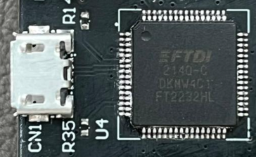
Figure 7- 2: FTDI Chip Located on the Board
Table 7- 1: JTAG/USB-UART Pin Assignment
|
FTDI Pin Name |
FPGA Pin Name |
FPGA Pin |
|
TCK |
TCK_0 |
L7 |
|
TMS |
TMS_0 |
M7 |
|
TDI |
TDI_0 |
N7 |
|
TDO |
TDO_0 |
N8 |
|
UART_TXD_IN |
IO_L6P_T0_15 |
D8 |
|
UART_RXD_OUT |
IO_L6N_T0_VREF_15 |
D9 |
8. User Input/Output Units
The TRUE-ARTDAC7 FPGA development board is equipped with various user input/output units to enable the implementation of fundamental digital design applications without the need for additional hardware. The board features 16 switches, 16 user LEDs, 5 push buttons, 1 RGB LED, 1 buzzer, and a 4-digit 7-segment display.
These peripherals allow for basic functions such as input reading, output driving, status indication, user interaction, audible alerts, and numerical data display to be performed directly on the board in FPGA-based designs. Consequently, users can rapidly develop and test logic circuits, counter applications, stopwatches, state machines, PWM-based control structures, and various verification scenarios.
The connections between the user I/O units on the board and the FPGA chip are shown in the following visuals.
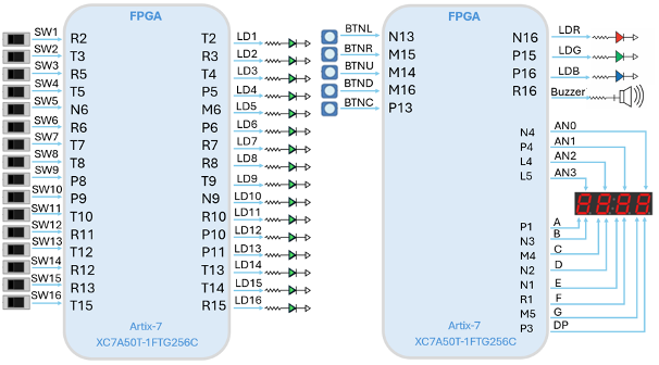
Figure 8- 1: Basic User Input/Output Connection Structure on the TRUE-ONE Board
Table 8- 1: User Input-Output Units Pin Assignment Table
|
Signal Name |
FPGA Pin Name |
Pin Assignment |
|
SW1 |
IO_L7P_T1_34 |
R2 |
|
SW2 |
IO_L9N_T1_DQS_34 |
T3 |
|
SW3 |
IO_L23P_T3_A03_D19_14 |
R5 |
|
SW4 |
IO_L23N_T3_A02_D18_14 |
T5 |
|
SW5 |
IO_L19N_T3_A09_D25_VREF_14 |
N6 |
|
SW6 |
IO_L24P_T3_A01_D17_14 |
R6 |
|
SW7 |
IO_L21P_T3_DQS_14 |
T7 |
|
SW8 |
IO_L21N_T3_DQS_A06_D22_14 |
T8 |
|
SW9 |
IO_L20P_T3_A08_D24_14 |
P8 |
|
SW10 |
IO_L18N_T2_A11_D27_14 |
P9 |
|
SW11 |
IO_L22N_T3_A04_D20_14 |
T10 |
|
SW12 |
IO_L17N_T2_A13_D29_14 |
R11 |
|
SW13 |
IO_L15N_T2_DQS_DOUT_CSO_B_14 |
T12 |
|
SW14 |
IO_L15P_T2_DQS_RDWR_B_14 |
R12 |
|
SW15 |
IO_L16P_T2_CSI_B_14 |
R13 |
|
SW16 |
IO_L10N_T1_D15_14 |
T15 |
|
LD1 |
IO_L8N_T1_34 |
T2 |
|
LD2 |
IO_L8P_T1_34 |
R3 |
|
LD3 |
IO_L9P_T1_DQS_34 |
T4 |
|
LD4 |
IO_L10P_T1_34 |
P5 |
|
LD5 |
IO_L19P_T3_A10_D26_14 |
M6 |
|
LD6 |
IO_25_14 |
P6 |
|
LD7 |
IO_L24N_T3_A00_D16_14 |
R7 |
|
LD8 |
IO_L20N_T3_A07_D23_14 |
R8 |
|
LD9 |
IO_L22P_T3_A05_D21_14 |
T9 |
|
LD10 |
IO_L18P_T2_A12_D28_14 |
N9 |
|
LD11 |
IO_L17P_T2_A14_D30_14 |
R10 |
|
LD12 |
IO_L14P_T2_SRCC_14 |
P10 |
|
LD13 |
IO_L14N_T2_SRCC_14 |
P11 |
|
LD14 |
IO_L16N_T2_A15_D31_14 |
T13 |
|
LD15 |
IO_L10P_T1_D14_14 |
T14 |
|
LD16 |
IO_L9P_T1_DQS_14 |
R15 |
|
BTNL |
IO_L11P_T1_SRCC_14 |
N13 |
|
BTNR |
IO_L3N_T0_DQS_EMCCLK_14 |
M15 |
|
BTNU |
IO_L4N_T0_D05_14 |
M14 |
|
BTND |
IO_L7P_T1_D09_14 |
M16 |
|
BTNC |
IO_L11N_T1_SRCC_14 |
P13 |
|
LDR |
IO_L7N_T1_D10_14 |
N16 |
|
LDG |
IO_L8P_T1_D11_14 |
P15 |
|
LDB |
IO_L8N_T1_D12_14 |
P16 |
|
Buzzer |
IO_L9N_T1_DQS_D13_14 |
R16 |
|
AN0 |
IO_L6N_T0_VREF_34 |
N4 |
|
AN1 |
IO_L5P_T0_34 |
P4 |
|
AN2 |
IO_L1P_T0_34 |
L4 |
|
AN3 |
IO_0_34 |
L5 |
|
7SEG_A |
IO_L4N_T0_34 |
P1 |
|
7SEG_B |
IO_L3P_T0_DQS_34 |
N3 |
|
7SEG_C |
IO_L1N_T0_34 |
M4 |
|
7SEG_D |
IO_L3N_T0_DQS_34 |
N2 |
|
7SEG_E |
IO_L4P_T0_34 |
N1 |
|
7SEG_F |
IO_L7N_T1_34 |
R1 |
|
7SEG_G |
IO_L6P_T0_34 |
M5 |
|
DP (Nokta) |
IO_L5N_T0_34 |
P3 |
9. Pin Header Structure and Expansion Infrastructure
The TRUE-ONE FPGA development board features various pin header structures designed for connecting external modules and user-defined peripherals. These headers provide users with direct access to the FPGA chip's input/output pins, enabling the development of diverse applications either as standalone projects or through integration with external hardware.
The board includes a total of four 2x6 and two 2x20 pin header structures. Through these headers, a total of 64 signals are routed to the FPGA chip. A portion of these signals serves as general-purpose input/output (GPIO), while another portion is dedicated specifically to the analog-to-digital converter architecture.
Specifically, 32 signals within the pin header structures are directly connected to the FPGA chip's analog input pins via the JXADC headers. This configuration allows users to leverage the FPGA's internal XADC infrastructure for monitoring, measuring, and processing analog signals. The remaining 32 signals are routed to general-purpose FPGA I/O pins, making them available for various digital design and communication applications.
In addition to the signal lines, the pin headers provide 3.3 V, 5 V, and GND connections. This setup simplifies the powering of external modules and facilitates organized signal routing. Consequently, the TRUE-ONE board functions as a flexible platform for education, R&D, prototyping, and experimental development, supported by both its onboard peripherals and its expansion capabilities. The schematic connections and physical pin layouts for the J1 and J2 headers are illustrated in the figures below.
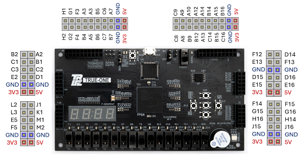
Figure 9- 1: TRUE-ONE Pin Header Pin Assignments
Table 9- 1: JXADC Pin Assignment Table
|
JXADC PIN |
Signal Name |
FPGA Pin Name |
Pin Assignment |
|
PIN1 |
+3V3 |
- |
- |
|
PIN2 |
GND |
- |
- |
|
PIN3 |
XADC1_P |
IO_L10P_T1_AD15P_35 |
E2 |
|
PIN4 |
XADC2_P |
IO_L7P_T1_AD6P_35 |
C3 |
|
PIN5 |
XADC3_P |
IO_L9P_T1_DQS_AD7P_35 |
C1 |
|
PIN6 |
XADC4_P |
IO_L8P_T1_AD14P_35 |
B2 |
|
PIN7 |
XADC4_N |
IO_L8N_T1_AD14N_35 |
A2 |
|
PIN8 |
XADC3_N |
IO_L9N_T1_DQS_AD7N_35 |
B1 |
|
PIN9 |
XADC2_N |
IO_L7N_T1_AD6N_35 |
C2 |
|
PIN10 |
XADC1_N |
IO_L10N_T1_AD15N_35 |
D1 |
|
PIN11 |
GND |
- |
- |
|
PIN12 |
+5V |
- |
- |
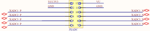
Figure 9- 2: TRUE-ONE JXADC Pin Header Connection Structure
Table 9- 1: JB Pin Assignment Table
|
JXADC PIN |
Signal Name |
FPGA Pin Name |
Pin Assignment |
|
PIN1 |
+3V3 |
- |
- |
|
PIN2 |
GND |
- |
- |
|
PIN3 |
JB1_P |
IO_L13P_T2_MRCC_35 |
F5 |
|
PIN4 |
JB1_N |
IO_L13N_T2_MRCC_35 |
E5 |
|
PIN5 |
JB2_P |
IO_L17P_T2_35 |
G2 |
|
PIN6 |
JB2_N |
IO_L17N_T2_35 |
G1 |
|
PIN7 |
JB4_N |
IO_L4N_T0_35 |
A3 |
|
PIN8 |
JB4_P |
IO_L4P_T0_35 |
B4 |
|
PIN9 |
JB3_N |
IO_L14N_T2_SRCC_35 |
F3 |
|
PIN10 |
JB3_P |
IO_L14P_T2_SRCC_35 |
F4 |
|
PIN11 |
GND |
- |
- |
|
PIN12 |
+5V |
- |
- |
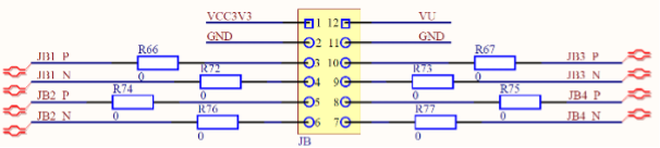
Figure 9- 3: TRUE-ONE JB Pin Header Connection Structure
Table 9- 1: JC Pin Assignment Table
|
JXADC PIN |
Signal Name |
FPGA Pin Name |
Pin Assignment |
|
PIN1 |
+3V3 |
- |
- |
|
PIN2 |
JC1 |
IO_L18N_T2_A23_15 |
E15 |
|
PIN3 |
JC2 |
IO_L15N_T2_DQS_ADV_B_15 |
D15 |
|
PIN4 |
GND |
- |
- |
|
PIN5 |
JC3 |
IO_L13N_T2_MRCC_15 |
E13 |
|
PIN6 |
JC4 |
IO_L16P_T2_A28_15 |
E12 |
|
PIN7 |
JC5 |
IO_L18P_T2_A24_15 |
F15 |
|
PIN8 |
JC6 |
IO_L16N_T2_A27_15 |
F13 |
|
PIN9 |
GND |
- |
- |
|
PIN10 |
JC7 |
IO_L17N_T2_A25_15 |
D16 |
|
PIN11 |
JC8 |
IO_L17P_T2_A26_15 |
E16 |
|
PIN12 |
+5V |
- |
- |
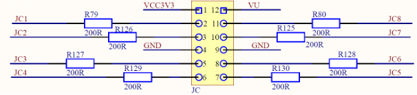
Figure 9- 4: TRUE-ONE JC Pin Header Connection Structure
Table 9- 1: JD Pin Assignment Table
|
JXADC PIN |
Signal Name |
FPGA Pin Name |
Pin Assignmen |
|
PIN1 |
+3V3 |
- |
- |
|
PIN2 |
GND |
- |
- |
|
PIN3 |
JD1 |
IO_L23P_T3_FOE_B_15 |
J15 |
|
PIN4 |
JD2 |
IO_L22P_T3_A17_15 |
H16 |
|
PIN5 |
JD3 |
IO_L24N_T3_RS0_15 |
G15 |
|
PIN6 |
JD4 |
IO_L21N_T3_DQS_A18_15 |
F14 |
|
PIN7 |
JD5 |
O_L18P_T2_A24_15 |
F15 |
|
PIN8 |
JD6 |
IO_L22N_T3_A16_15 |
G16 |
|
PIN9 |
JD7 |
IO_L24P_T3_RS1_15 |
H14 |
|
PIN10 |
JD8 |
IO_L23N_T3_FWE_B_15 |
J16 |
|
PIN11 |
GND |
- |
- |
|
PIN12 |
+5V |
- |
- |
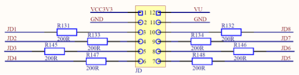
Figure 9- 5: TRUE-ONE JD Pin Header Connection Structure
Table 9- 1: JXADC Pin Assignment Table
|
JXADC PIN |
Signal Name |
FPGA Pin Name |
Pin Assignment |
|
PIN1 |
+3V3 |
- |
- |
|
PIN2 |
GND |
- |
- |
|
PIN3 |
XADC9_P |
IO_L10P_T1_AD11P_15 |
C16 |
|
PIN4 |
XADC10_P |
IO_L9P_T1_DQS_AD3P_15 |
B15 |
|
PIN5 |
XADC11_P |
IO_L8P_T1_AD10P_15 |
C14 |
|
PIN6 |
XADC12_P |
IO_L7P_T1_AD2P_15 |
A13 |
|
PIN7 |
XADC13_P |
IO_L5P_T0_AD9P_15 |
B12 |
|
PIN8 |
XADC14_P |
IO_L3P_T0_DQS_AD1P_15 |
B9 |
|
PIN9 |
XADC15_P |
IO_L2P_T0_AD8P_15 |
A8 |
|
PIN10 |
XADC16_P |
IO_L1P_T0_AD0P_15 |
C8 |
|
PIN11 |
XADC16_N |
IO_L1N_T0_AD0N_15 |
C9 |
|
PIN12 |
XADC15_N |
IO_L2N_T0_AD8N_15 |
A9 |
|
PIN13 |
XADC14_N |
IO_L3N_T0_DQS_AD1N_15 |
A10 |
|
PIN14 |
XADC13_N |
IO_L5N_T0_AD9N_15 |
A12 |
|
PIN15 |
XADC12_N |
IO_L7N_T1_AD2N_15 |
A14 |
|
PIN16 |
XADC11_N |
IO_L8N_T1_AD10N_15 |
B14 |
|
PIN17 |
XADC10_N |
IO_L9N_T1_DQS_AD3N_15 |
A15 |
|
PIN18 |
XADC19_N |
IO_L10N_T1_AD11N_15 |
B16 |
|
PIN19 |
GND |
- |
- |
|
PIN20 |
+ 5V |
- |
- |
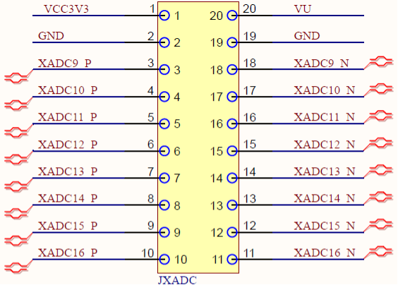
Figure 9- 6: TRUE-ONE JXADC Pin Header Connection Structure
Table 9- 1: JA Pin Assignment Table
|
JXADC PIN |
Signal Name |
FPGA Pin Name |
Pin Assignment |
|
PIN1 |
+3V3 |
- |
- |
|
PIN2 |
GND |
- |
- |
|
PIN3 |
XADC5_P |
IO_L1P_T0_AD4P_35 |
B7 |
|
PIN4 |
XADC6_P |
IO_L5P_T0_AD13P_35 |
C7 |
|
PIN5 |
XADC7_P |
IO_L2P_T0_AD12P_35 |
B6 |
|
PIN6 |
XADC8_P |
IO_L3P_T0_DQS_AD5P_35 |
A5 |
|
PIN7 |
JA4_P |
IO_L4P_T0_35 |
B4 |
|
PIN8 |
JA3_P |
IO_L14P_T2_SRCC_35 |
F4 |
|
PIN9 |
JA2_P |
IO_L17P_T2_35 |
G2 |
|
PIN10 |
JA1_P |
IO_L20P_T3_35 |
H2 |
|
PIN11 |
JA1_N |
IO_L20N_T3_35 |
H1 |
|
PIN12 |
JA2_N |
IO_L17N_T2_35 |
G1 |
|
PIN13 |
JA3_N |
IO_L14N_T2_SRCC_35 |
F3 |
|
PIN14 |
JA4_N |
IO_L4N_T0_35 |
A3 |
|
PIN15 |
XADC8_N |
IO_L3N_T0_DQS_AD5N_35 |
A4 |
|
PIN16 |
XADC7_N |
IO_L2N_T0_AD12N_35 |
B5 |
|
PIN17 |
XADC6_N |
IO_L5N_T0_AD13N_35 |
C6 |
|
PIN18 |
XADC5_N |
IO_L1N_T0_AD4N_35 |
A7 |
|
PIN19 |
GND |
- |
- |
|
PIN20 |
+ 5V |
- |
- |
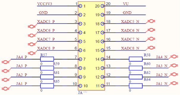
Figure 9- 7: TRUE-ONE JA Pin Header Connection Structure
10. Block Diagram
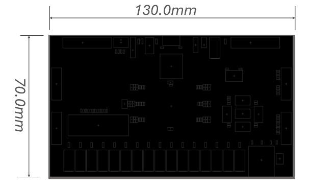
Figure 10- 1: Top Dimensional View of the TRUE-ONE Board